Home | About | Apps | Github | Rss
Automated Plant Watering System - Part 2 - PCB Design and Prototyping
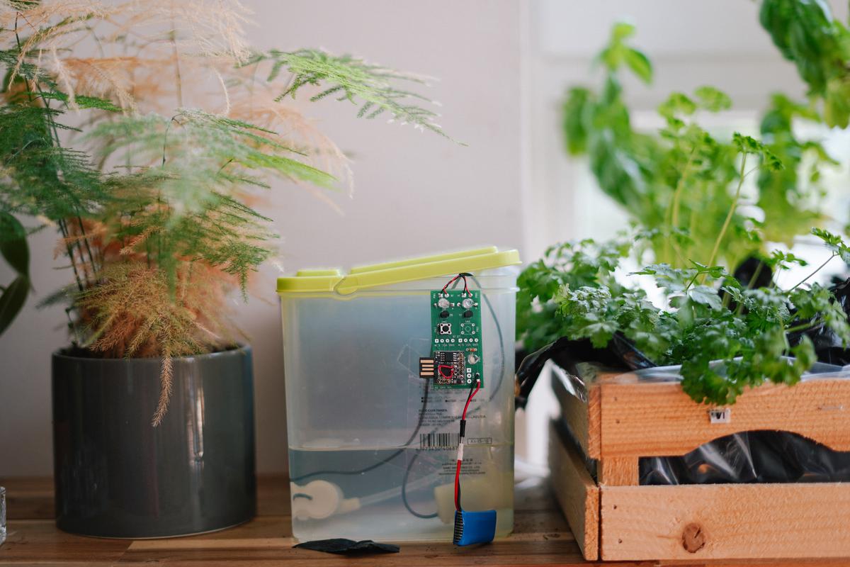
After running the Mark-1 prototype for a week, I wanted to scale up this effort for more of my plants. However efforts to prototype on a PCB blank were a complete mess, so I decided to jump the gun and build Mark-2.
Mark-2 Design Goals:
It was clear that running one MCU per plant was not effective, at the same time I wanted configurability and thus compromises had to be made.
- Run on AA batteries or 3.7v LiPo cells.
- Control at least 2 Motors
- Configure using 2 push buttons with ability to bypass it to use other peripherals such as a soil sensor.
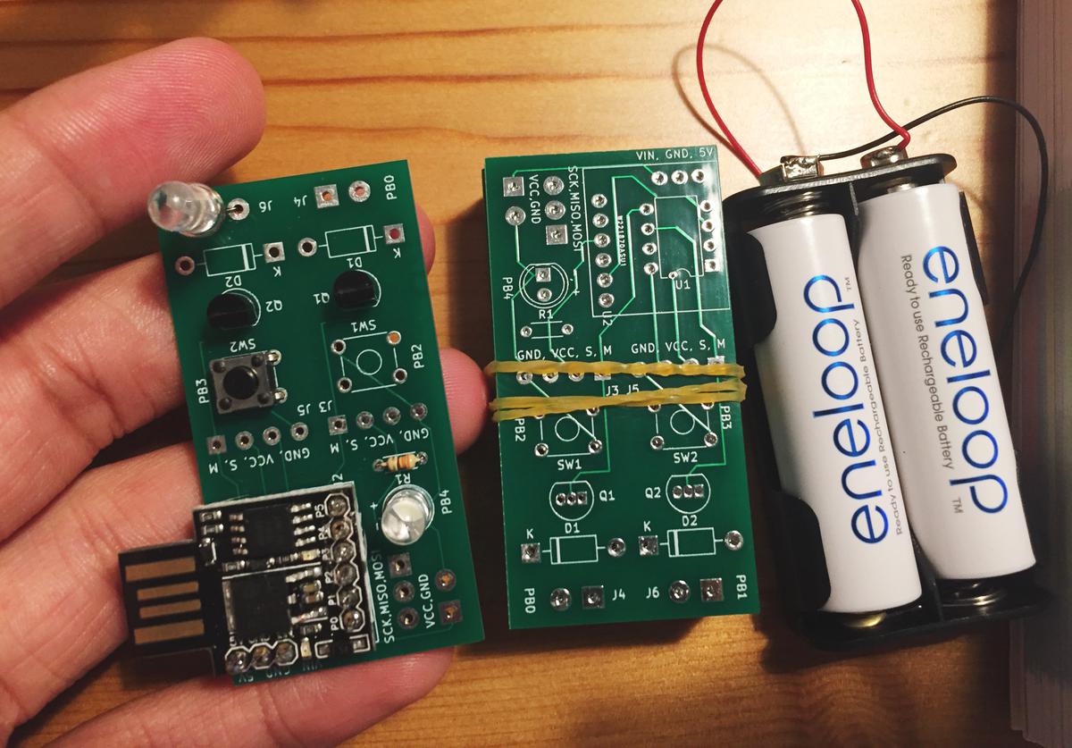
- Accommodate both Attiny85 bare IC as well as Digispark.
Bill of materials:
- Digispark Attiny85 or bare IC.
- 2x NPN Transistors (I used BC547 at hand)
- 2x Diodes (I used LEDs due to lack of proper diodes)
- 2x 3v Submersible DC Pumps
- 1x LED for feedback display
- 1x battery pack (min 3v)
Design
Design was fairly similar to earlier prototype with just few more ports.
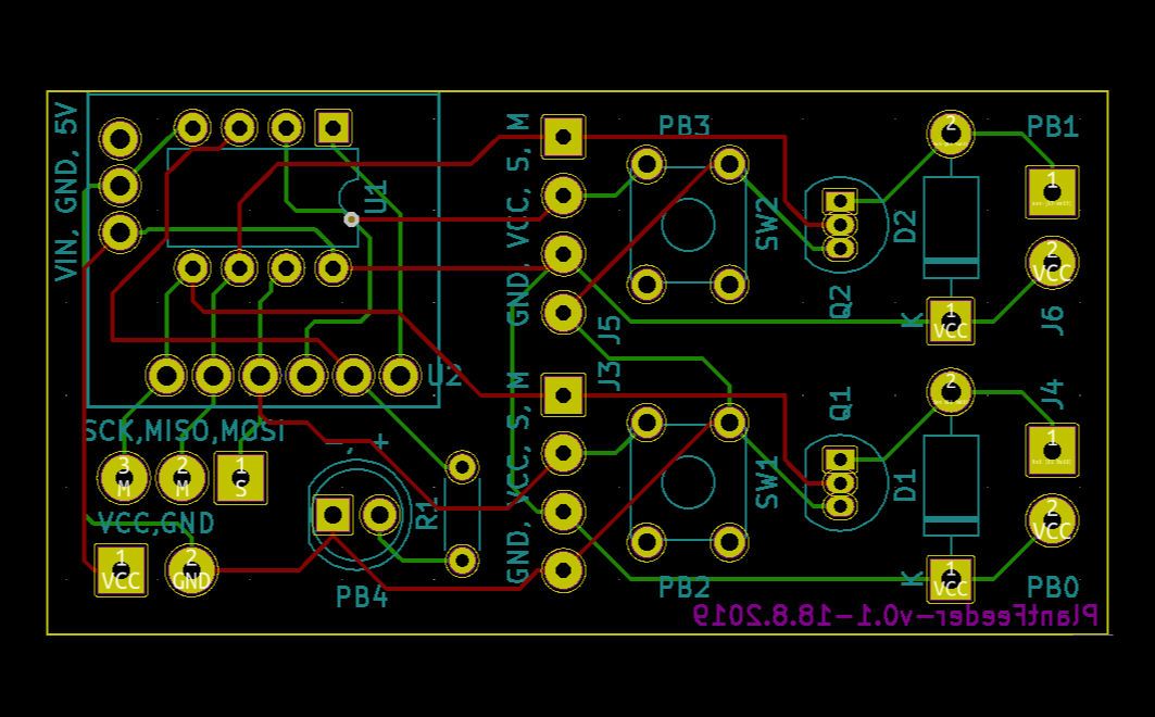
The design phase involved both schematic design as well as PCB footprint design using KiCad. I made use of hierarchical sheets to “re-use” the schematic design for a single motor.
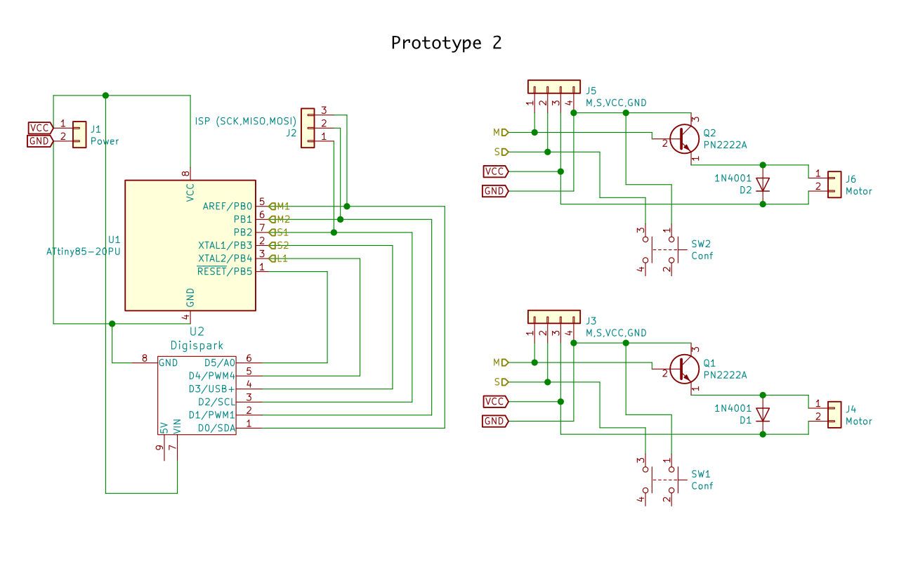
I used the “Save/Restore Layout” plugin to do the same in PCB mode.
Program
It turned out that the use of a push button without a pull down resistor makes it unusable, due to which am now relying on manual programming.
The duration is programmed to be 2 seconds of watering for every 2 hours, which appears to be adequate for my basil and coriander plants
The code itself was similar to earlier version.
PCB Fabrication
The final step was to export Gerber files, containing Image/SVG representation of all individual layers such as copper front and back, silkscreen for info, soldermask, vias, etc.
A key element of design that I missed during first iteration was the edge cuts which is the SVG layer outlining how the PCB has to be cut.
All the exported files were zipped and sent to pcbway. The fabbed PCBs arrived less than a week later. As shipping was the most expensive part of the process, I might perhaps combine multiple designs into a PCB order so they arrive together.
KiCad Note:
Install plugins by copying files from
- Source:
https://github.com/MitjaNemec/Kicad_action_plugins.git - Destination (macOS):
/Applications/KiCad/kicad.app/Contents/SharedSupport/scripting/plugins/
More posts
- Next: Stuff I learnt in 2019
- Previous: Automated Plant Watering System - Part 1